
セミナー情報
CPEC seminar
CPEC seminar
日 時: |
2018年2月20日(火) 14:00 - 15:00 | 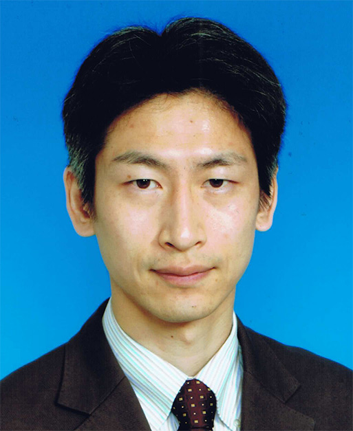 |
会 場: |
東京大学駒場リサーチキャンパス 生産技術研究所 C棟ラウンジ | |
問合せ先: |
東京大学生産技術研究所内 光電子融合研究センター事務局 電話: 03-5452-6281, E-mail: cpec[at]iis.u-tokyo.ac.jp |
|
講 師: |
久保 敦 氏 (筑波大学数理物質系・物理学域 講師) | |
タイトル: |
フェムト秒時間領域における表面プラズモン波束の動的振舞い Dynamical behavior of surface plasmon wavepacket in femtosecond time-domain. |
|
Abstract: |
表面プラズモンポラリトン(SPP)は10-100 fs程度のコヒーレンス寿命を有するが、その間の性質は、波の干渉・回折を示し分散関係に従った位相速度・群速度で伝搬するなど、光波と類似する。このため、分散による包絡線形状の変形、遅い光・速い光、負の群速度、異常屈折など、光波に見られる多彩な伝搬特性はSPPにもあてはまる。 講演では、フェムト秒時間分解顕微鏡法を用いて取得されるSPP波束伝搬の動画像と、そこから帰結される波束の動的特性について議論する。また、人工的なナノ構造(メタ原子)との相互作用で生じる波束の変調についても紹介する。 |
|
CPEC seminar
CPEC seminar
日 時: |
2017年3月9日(木) 13:30 - 15:00 | 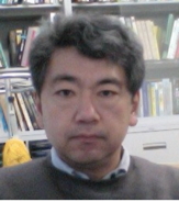 |
会 場: |
東京大学駒場リサーチキャンパス 生産技術研究所 中セミナー室1 (An401/402) | |
問合せ先: |
東京大学生産技術研究所内 光電子融合研究センター事務局 電話: 03-5452-6281, E-mail: cpec[at]iis.u-tokyo.ac.jp |
|
講 師: |
初貝 安弘 氏 (筑波大学数理物質系・物理学域 教授) | |
タイトル: |
トポロジカル相におけるバルク・エッジ対応と応用への期待 | |
Abstract: |
近年話題のトポロジカル相は歴史的には量子ホール効果をその起源とするが、今日ではトポロジカルな現象は電子系固有のものではなく、さらに量子力学も必須の要件とせず、誘電体中の光や固体の振動等の古典力学系にも適用される普遍的な現象であると考えられている。その特徴は系の境界や不純物、欠陥などの近傍に存在する局在状態(エッジ状態)の存在にある。この広義の「エッジ状態」はバルクのエネルギーギャップにより「トポロジカルに」保護され、外乱や形状の乱れ等に対する高い安定性を持ち、それゆえ潜在的に大きな応用の可能性を持つ。時間反転対称性を破るメタマテリアル中の光のカイラルな伝搬モードや超伝導体中のマヨラナ粒子等がその典型例である。 講演では、種々の具体的な現象におけるエッジ状態の紹介から始めて、そのエッジ状態を「バルク・エッジ対応」としての一般的な観点から(感覚的に)理解することを目指す。また、時間の許す限り背景となる関連の物理に関しても予備知識を仮定せず紹介したい。 |
|
CPEC seminar
CPEC seminar
日 時: |
2017年1月23日(月) 14:00 - | 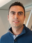 |
会 場: |
東京大学駒場リサーチキャンパス 生産技術研究所 E棟ラウンジ | |
問合せ先: |
東京大学生産技術研究所内 光電子融合研究センター事務局 電話: 03-5452-6281, E-mail: cpec[at]iis.u-tokyo.ac.jp |
|
講 師: |
Dr. Luca Sapienza (Department of Physics & Astronomy, University of Southampton, UK) | |
タイトル: |
On-chip nanophotonics: controlling light at the single photon level |
|
Abstract: |
Solid-state quantum emitters are required for quantum information protocols relying on the storage, manipulation, and transmission of the information encoded in single photons through optical cavities and waveguides. Semiconductor quantum dots are particularly promising quantum light sources that can allow both the investigation of fundamental physics phenomena on a chip and quantum technology applications. I will discuss the implementation of quantum dot nanostructures to create simultaneously bright and pure, on-demand, single-photon sources in engineered nanophotonic devices in gallium arsenide and hybrid silicon/III-V materials. I will present different photonic geometries for controlling light propagation, brightness and spontaneous emission rate, based on circular grating and ring cavities. Finally, I will focus on the comparison between highly engineered structures and disordered photonic crystal waveguides, showing efficient light confinement and optical sensing on a silicon nitride platform in the visible range of wavelengths. |
|
CPEC seminar
CPEC seminar
日 時: |
2016年5月18日(水) 13:00 - 14:00 | 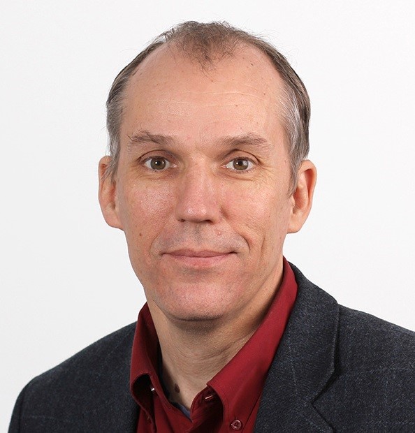 |
会 場: |
東京大学駒場リサーチキャンパス 生産技術研究所 E棟ラウンジ | |
問合せ先: |
東京大学生産技術研究所内 光電子融合研究センター事務局 電話: 03-5452-6281, E-mail: cpec[at]iis.u-tokyo.ac.jp |
|
講 師: |
Prof. Axel Lorke (University of Duisburg-Essen, Germany) | |
タイトル: |
Electronic and optical properties of quantum dots | |
Abstract: |
Decades of improvement in fabrication and synthesis techniques have enabled us today to realize nanometer-scale devices, which make use of tailored, size and shape-dependent properties. The most striking size effects are based on quantum properties in semiconductor nanostructures, such as quantum wells, quantum wires, and quantum dots. Quantum dots are the solid-state equivalent of atoms, with properties like a shell structure, Coulomb and exchange interaction, optical transitions and the Zeeman effect. This makes them fascinating study objects for basic science - but also promising building blocks for both visionary future devices and present-day applications. Indeed, tailored quantum dots can be found today in consumer products such as LCD television screens. In this talk, some basic properties of quantum dots will be reviewed, using self-assembled InAs nano-islands as a model system. It will be discussed how fundamental investigations of their properties can lead to an understanding of the inner workings of quantum dots that can help improve the efficiency of nanoparticles used for commercial applications. |
|
CPEC seminar
CPEC seminar
日 時: |
2016年4月11日(月) 14:00 - 15:00 | 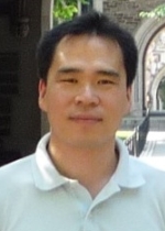 |
会 場: |
東京大学駒場リサーチキャンパス 生産技術研究所 E棟ラウンジ | |
問合せ先: |
東京大学生産技術研究所内 光電子融合研究センター事務局 電話: 03-5452-6281, E-mail: cpec[at]iis.u-tokyo.ac.jp |
|
講 師: |
Dr. Minkyung Jung (Department of Physics, University of Basel, Switzerland) | |
タイトル: |
Ultraclean carbon nanotube quantum dots coupled to superconducting impedance matching circuits + InAs charge pump |
CPEC seminar
CPEC seminar
日 時: |
2016年3月24日(木) 14:00 - 15:30 | 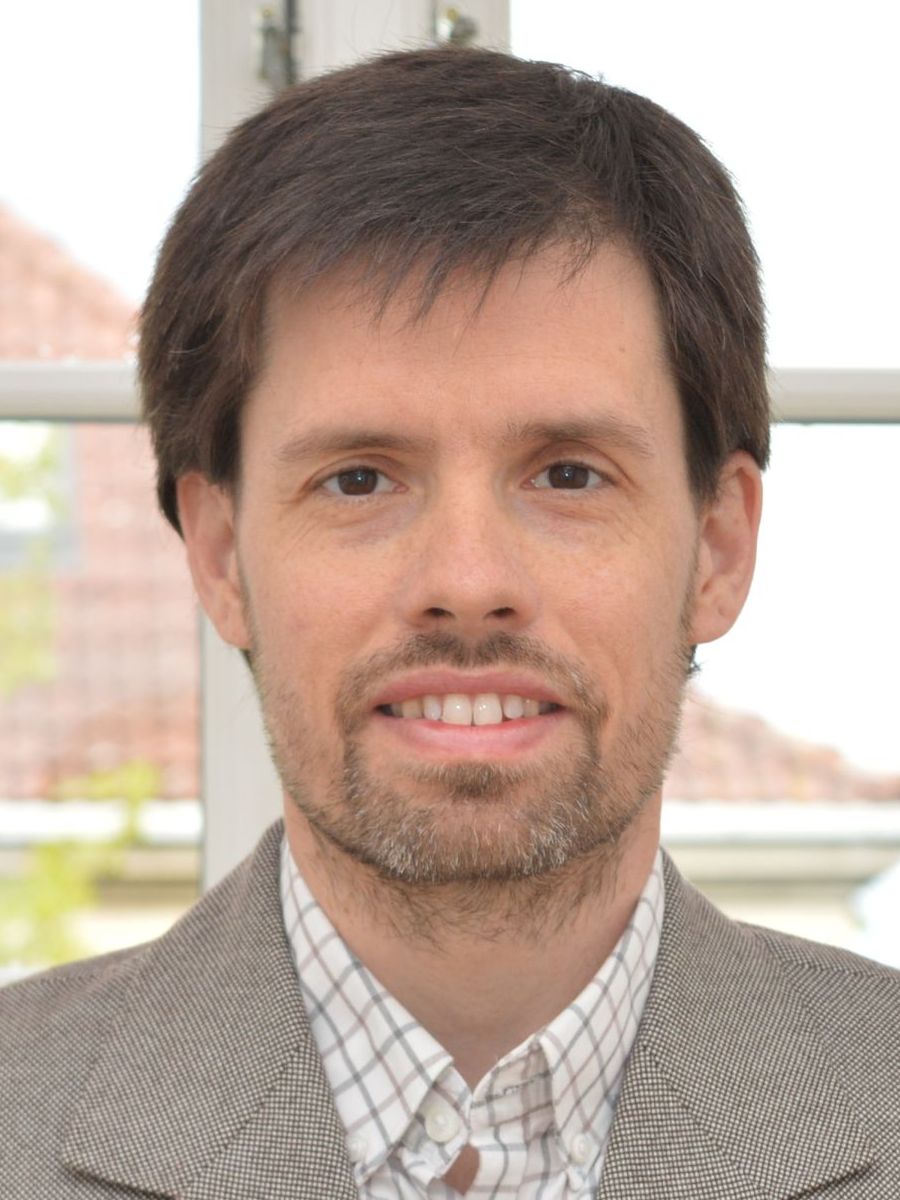 |
会 場: |
東京大学駒場リサーチキャンパス 産学連携活動室(Dw404) | |
問合せ先: |
東京大学生産技術研究所内 光電子融合研究センター事務局 電話: 03-5452-6281, E-mail: cpec[at]iis.u-tokyo.ac.jp |
|
講 師: |
Dr. Morten Bache (Department of Photonics Engineering, Technical University of Denmark, Denmark) | |
タイトル: |
Ultrashort and broadband mid-IR pulses: challenges and solutions | |
Abstract: |
A current challenge is generating bright, coherent and broadband mid-IR laser pulses. I will present various soliton-based techniques where the soliton can become phase-matched in the mid-IR by so-called resonant radiation (dispersive wave formation). For a negative nonlinearity soliton this occurs in bulk media (e.g. quadratic nonlinear crystals), while for a standard positive nonlinearity soliton it requires substantial waveguide dispersion. I will show experiments in lithium niobate (LN), periodically poled LN, and silicon-based CMOS compatible waveguides, all having substantial mid-IR content. Many applications also require ultrashort few-cycle laser pulses, and I will show a new mid-IR external pulse-compression technique. | |
CPEC seminar
CPEC seminar
日 時: |
2016年2月19日(金) 16:00 - 17:30 |  |
会 場: |
東京大学駒場リサーチキャンパス 中セミナー室4 (As311/312) | |
問合せ先: |
東京大学生産技術研究所内 光電子融合研究センター事務局 電話: 03-5452-6281, E-mail: cpec[at]iis.u-tokyo.ac.jp |
|
講 師: |
小川 直毅 氏 (理化学研究所 創発物性科学研究センター(CEMS) 創発光物性研究ユニット) |
|
タイトル: |
Optical control of magnetic skyrmions and bubbles | |
Abstract: |
Magnetic skyrmions, particle-like spin textures of topological origin, have been identified in several magnetic materials. We study the dynamics of these skyrmions by using time-resolved magneto-optics. In a chiral magnet Cu2OSeO3, helimagnons and three collective modes of the skyrmion have been excited by the inverse-Faraday effect. In iron garnet films, magnetic bubbles were manipulated by the photoexcited magnetoelastic waves. | |
CPEC seminar
CPEC seminar
日 時: | 2015年9月2日(水) 16:00 - 16:50 |  |
会 場: | 東京大学駒場リサーチキャンパス(Dw-404) |
|
問合せ先: | 東京大学生産技術研究所内 光電子融合研究センター事務局 電話: 03-5452-6281, E-mail: cpec[at]iis.u-tokyo.ac.jp |
|
講 師: | Prof.Yang Tian (East China Normal University, China) |
|
タイトル: | Bioimaging and Biosensing of Reactive Oxygen Species and Related Species in Living Cells |
|
CPEC seminar
CPEC seminar
日 時: | 2015年9月2日(水) 13:30 - 15:00 | 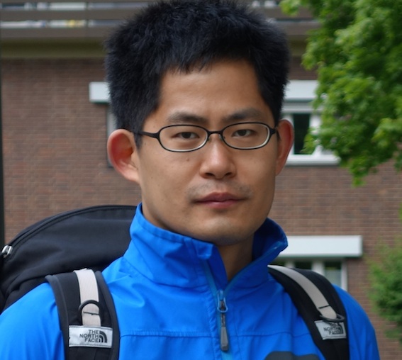 |
会 場: | 東京大学駒場リサーチキャンパス産学連携活動室(Dw404) |
|
問合せ先: | 東京大学生産技術研究所内 光電子融合研究センター事務局 電話: 03-5452-6281, E-mail: cpec[at]iis.u-tokyo.ac.jp |
|
講 師: | Dr. Sho Imoto (Lehrstuhl für Theoretische Chemie, Ruhr-Universität Bochum, Germany) |
|
タイトル: | Ultrafast Dynamics of Liquid Water: Energy Relaxation and Transfer Processes of the OH Stretch and the HOH Bend |
|
Abstract: | 水中におけるエネルギー散逸は他の溶液に比べて速く、また非常に複雑であることが知られている。我々は特に水のOH伸縮振動とHOH変角振動に注目し、高精度な水の力場と非平衡分子動力学を用いることで励起による余剰エネルギーがどのように散逸するのか理論的解析を行った。 | |
CPEC seminar
CPEC seminar
日 時: | 2015年7月24日(金) 17:00 - 18:00 | 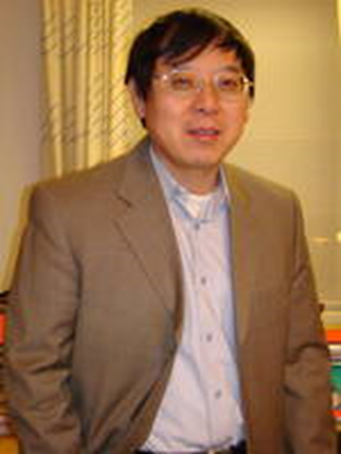 |
会 場: | 東京大学駒場リサーチキャンパス(E-Lounge) |
|
問合せ先: | 東京大学生産技術研究所内 光電子融合研究センター事務局 電話: 03-5452-6281, E-mail: cpec[at]iis.u-tokyo.ac.jp |
|
講 師: | Prof. Hongqi Xu (Peking University, China, and Lund University, Sweden) |
|
タイトル: | Majorana fermions in topological superconducting nanowires |
|
Abstract: | The search for Majorana fermions in solid state systems is one of paramount research tasks in physics today. Majorana fermions are an elusive class of fermions that are their own antiparticles. Although an extensive effort has been made worldwide in particle physics, Majorana fermions have so far not been convincingly discovered in free space. In recent years, numerous proposals for probing Majorana fermion states in solid state systems have been suggested. The most recent ones are to explore a topological superconductor phase of a strong spin−orbit coupled semiconductor nanowire in the proximity of an s-wave superconductor. These proposals have stimulated a new wave of search for Majorana fermions in solid state systems. Here I report on experimental observations of the signatures of Majorana fermions in topological superconducting nanowire quantum devices made from high crystal-quality InSb nanowires and superconductor Nb contacts. | |
CPEC seminar
CPEC seminar
日 時: | 2015年7月22日(水) 10:30 - 11:30 |  |
会 場: | 東京大学駒場リサーチキャンパス(Dw-404) |
|
問合せ先: | 東京大学生産技術研究所内 光電子融合研究センター事務局 電話: 03-5452-6281, E-mail: cpec[at]iis.u-tokyo.ac.jp |
|
講 師: | Prof. Zhongfan Liu (Peking University, China) |
|
タイトル: | Graphene and beyond: Attraction, Reality and Future |
CPEC seminar
CPEC seminar
日 時: | 2015年2月19日(木) 10:00~11:00 |  |
会 場: | 東京大学駒場リサーチキャンパス(Dw-404) |
|
問合せ先: | 東京大学生産技術研究所内 光電子融合研究センター事務局 電話: 03-5452-6281, E-mail: cpec[at]iis.u-tokyo.ac.jp |
|
講 師: | Prof. Nathalie Destouches (Université de Lyon - Université Jean Monnet, France) |
|
タイトル: | Self-organization and plasmonic hybridization of metal nanoparticle ensembles |
|
Abstract: | TExciting the plasmon resonance of silver nanoparticles (NPs) embedded in a TiO2 thin film with a visible laser scanning the film surface can give rise to an interesting self-organization process. The latter leads to the generation of waveguiding metallic photonic crystals made of periodic nanoparticle arrays buried in the film, which exhibit singular optical properties. Their generation is a complex process involving various physico-chemical mechanisms, which are shown to be driven by both radiative and non-radiative decays of the localized surface plasmon resonance of Ag NPs. Charge transfers from metallic NPs to the semiconductor TiO2 matrix, through the Schottky junction, and the material heating result in two opposite effects that are the shrinkage or the growth of silver nanoparticles through oxidation or reduction/growth reactions, respectively. Coupled mode modeling to interpret hybrid modes and Fano resonances in plasmonic systems is also described. | |
CPEC seminar
CPEC seminar
日 時: | 2015年1月30日(金) 13:00~14:00 |  |
会 場: | 東京大学駒場リサーチキャンパス(As303/304) |
|
問合せ先: | 東京大学生産技術研究所内 光電子融合研究センター事務局 電話: 03-5452-6281, E-mail: cpec[at]iis.u-tokyo.ac.jp |
|
講 師: | Prof. Gerhard Abstreiter (Walter Schottky Institut and Institute for Advanced Study, TU Muenchen, 85748 Garching, Germany) |
|
タイトル: | GaAs based hetero-nanowires for nanophotonics and
nanolelectronics applications |
|
Abstract: | Semiconductor nanowires (NWs) are widely considered as next frontier in the drive towards smaller and versatile nanophotonic and nanoelectronic devices. III-V nanowires can be combined with CMOS compatible technologies and provide much promise for future nanoelectronics as well as the efficient delivery of light, the exploration of new regimes of optical signal processing and even sensing with ultrahigh detectivity. This is made possible especially with sophisticated core shell hetero-NW geometries. Here we report on epitaxial growth of complex Ga(In)As based core-shell NWs on pre-patterned Si substrates. The light emission can be tuned from about 1.6 eV down to about 0.4 eV, depending on composition and NW diameter, thus covering also the wavelength regime for optical fiber communication. The luminescence efficiency is increased by several orders of magnitude when the nanowires are passivated with thin shells consisting of AlGaAs in the case of Ga rich NWs, InAlAs in the intermediate concentration regime and InAsP in the case of In rich NWs. In this way we have achieved optically pumped infrared lasing up to room temperature from individual GaAs-AlGaAs core shell NWs with remarkably low threshold pump power densities. Our results show that by carefully designing NW materials composition profile high performance III-V near infrared NW lasers can be directly grown on Si substrates and thus open a path towards infrared photonic and optoelectronic applications on a Si platform. In addition, remote doping of the shell also leads to high mobility 2d and 1d channels in the core which are basis for novel NW field effect transistors. This work was performed in close collaboration with Jonathan Finley and Gregor Koblmüller together with various PhD- and Masterstudents at the Walter Schottky Institute of TUM. We acknowledge financial support from the Deutsche Forschungsgemeinschaft via SFB 631, the cluster of excellence “Nanosystems Intiative Munich”, and the Focus group “Nanophotonics” of the TUM Institute for Advanced Study. | |
CPEC seminar
CPEC seminar
日 時: | 2014年12月3日(水) 16:00~17:00 |  |
会 場: | 東京大学駒場リサーチキャンパスSeminar room 5 (As313/314) |
|
問合せ先: | 東京大学生産技術研究所内 光電子融合研究センター事務局 電話: 03-5452-6281, E-mail: cpec[at]iis.u-tokyo.ac.jp |
|
講 師: | Paulo Santos (Senior Scientist, Paul-Drude-Institut für Festkörperelektronik, Germany) |
|
タイトル: | Control of excitons and exciton-polariton condensates by acoustic lattices |
|
Abstract: | The tunable strain field of a surface acoustic waves (SAW) provides an excellent tool for the manipulation and transport of excitonic systems in semiconductors. We report on the transport of excitons as well as on the modulation of microcavity exciton-polariton condensates by acoustic lattices. The latter leads to the formation of very regular arrays of confined condensates with controlled inter-site coupling, which are solid-state analogues of optical lattice of cold atoms. We show that the lattices exhibit strong non-linearities, including solitonic behavior, thus providing a test bed for the investigation of many body interactions in non-equilibrium quantum phases. | |
CPEC seminar
CPEC seminar
日 時: | 2014年11月13日(木) 11:00~12:00 |  |
会 場: | 東京大学駒場リサーチキャンパス E-lounge |
|
問合せ先: | 東京大学生産技術研究所内 光電子融合研究センター事務局 電話: 03-5452-6281, E-mail: cpec[at]iis.u-tokyo.ac.jp |
|
講 師: | prof. Gerald Bastard, Ecole Normale Superieure |
|
タイトル: | Inter-subband lineshape in lightly doped quasi 2D heterostructuress |
|
Abstract: | We report on intersubband lineshape in imperfect quasi 2D heterostructures that contain few carriers (a few 1010cm-2) as it is realised in e. g. Quantum Cascade Lasers. This allows neglecting many body effects such as the depolarisation shifts. Impurities, interface defects are considered in the lineshape calculations. We find that different mechanisms (intra-subband versus inter-subband scatterings) control the tails and the centre of the line. We shall also show that bound states created by the impurities/defects may give rise to extra absorption peaks (impurity inter-subband absorption). These peaks have been observed both in Quantum Wells and in superlattice structures. | |
CPEC seminar
CPEC seminar
日 時: | 2014年10月24日(金) 17:00~18:00 |
会 場: | 東京大学駒場リサーチキャンパス E-lounge |
問合せ先: | 東京大学生産技術研究所内 光電子融合研究センター事務局 電話: 03-5452-6281, E-mail: cpec[at]iis.u-tokyo.ac.jp |
講 師: | Prof. Alwyn Seeds (University College London, UK) |
タイトル: | III-V Quantum-Dot Lasers Monolithically Grown on Si Substrates |